There are several key players in the AI computing infrastructure landscape, but there are emerging new players with custom design AI compute chips, each with their own strengths and preferences in terms of hardware. Here’s a breakdown of some leaders and their chip focus:
Cloud-based AI platforms
- Google Cloud: Google has its own Tensor Processing Unit (TPU) specifically designed for AI workloads, offering high performance and efficiency. They also use Nvidia GPUs and custom CPUs in their cloud offerings.
- Amazon Web Services (AWS): AWS offers a variety of AI hardware options, including Nvidia GPUs, custom AWS Inferentia chips for inference tasks, and FPGAs. They also leverage Intel and AMD CPUs for general-purpose AI workloads.
- Microsoft Azure: Azure utilizes Nvidia GPUs and its own Field Programmable Gate Arrays (FPGAs) for AI training and inference. Additionally, they have their own line of Azure Machine Learning chips focusing on edge computing applications.
- IBM Cloud: IBM relies on Nvidia GPUs and its own Power architecture CPUs for AI computations. Additionally, they develop and utilize specialized neuromorphic chips like TrueNorth for specific applications.
Hardware and chip manufacturers
- Nvidia: Nvidia is a dominant player in the AI hardware space, with their powerful and versatile GPUs being the go-to choice for many AI tasks. They also offer dedicated AI accelerators like the DGX A100 system.
- Intel: Intel offers a range of CPUs and AI accelerators, including Xeon CPUs with built-in AI features and dedicated AI chips like Habana Labs Deep Learning Processor (HLDP).
- AMD: Similar to Intel, AMD provides CPUs with AI-optimized features and dedicated AI accelerators like Alveo FPGAs.
- Arm: Arm processors are increasingly popular for edge computing applications due to their lower power consumption. Many chipmakers create Arm-based SoCs with AI capabilities for devices like smartphones and IoT devices.
Noteworthy New Players To Watch
- Tesla: Tesla’s custom AI chips developed for Autopilot and FSD systems are also being incorporated into various AI applications.
- Xilinx: Xilinx provides FPGAs for AI acceleration, offering flexibility and customization for specific tasks.
- Cerebras Systems have developed their own custom AI chip
The landscape of AI computing infrastructure is constantly evolving, with new players and technologies emerging. Ultimately, the choice of leaders and chip types depends on specific needs and applications. Some considerations include:
- Performance: Different chips offer varying levels of performance for different AI tasks.
- Cost: Costs can vary greatly depending on the type of hardware and cloud services chosen.
- Development ecosystem: Some platforms and chips offer more mature and user-friendly development environments.
- Sustainability: Considerations like energy efficiency and power consumption are becoming increasingly important.
By understanding the strengths and offerings of different leaders and chip types, you can make informed decisions about your AI computing infrastructure needs.
Custom Design AI Chip from Cerebras
The custom chip from Cerebras is
- Full wafer size (not chopped up)
- 5nm from TSMC
- 850,000 cores
- Every core single-clock-cycle access to fast memory at extremely high bandwidth – 20 PB/s. This is 1,000x more capacity and 9,800x greater bandwidth than the leading GPU.
- 220Pb/s memory to memory fabric.

| Feature | WSE-2 | A100 | |
| Chip Size | 46,225 mm2 | 826 mm2 | 56 X |
| Cores | 850,000 | 6912 + 432 | 123X |
| On-chip memory | 40 Gigabytes | 40 Megabytes | 1,000 X |
| Memory bandwidth | 20 Petabytes/sec | 1.6 Terabytes/sec | 12,733 X |
| Fabric bandwidth | 220 Petabits/sec | 4.8 Terabits/sec | 45,833 X |
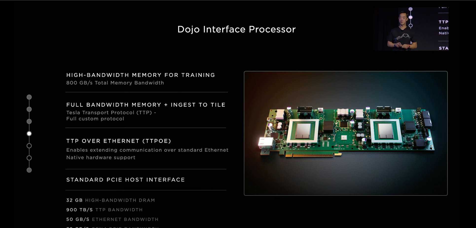
Tesla’s Dojo – Another Custom Design
The architectural uniqueness of Dojo is evident in its building block, the D1 chip, manufactured by TSMC using 7 nm semiconductor nodes, with a large die size of 645 mm² and 50 billion transistors and leveraging a RISC-V approach and custom instructions. Tesla claims a die with 354 Dojo cores can hit 362 BF16 TFLOPS at 2 GHz, indicating that each core can do 512 BF16 FLOPS per cycle.
The interface is 2×512 and connects directly to other Dojo Chips in a single cabinet. See below for further transmission advances. In their earnings call in July 2024, Tesla stated they were continuing their inhouse development as they needed a second source of AI chips as NVidia was so much in demand the company could find itself without the computing capacity they needed, and also stated that DOJO was as good as or even better than NVidia’s offering.

Comparison with Other AI Chips
Design is for AI training compute efficiency. Enables 362Tflops or 6 to 10 times more than other AI.
| Tesla Dojo D1 Chip | Fujitsu A64FX | AMD RX 6900 XT | IBM Cell | |
| Area (die) | 645 mm2 | ~400 mm2 | 520 mm2 | ~235 mm2 |
| Process Node | TSMC 7 nm | TSMC 7 nm | TSMC 7 nm | IBM 90 nm SOI, later shrink to 65nm |
| Core area, approx | 1.1 mm2 | 3.08 mm2 | 14.8 mm2 | |
| Core Count | 354 | 48+4 | 40 WGPs | 8 SPE + 1 PPE |
| Core Clock Speed | 2 GHz | 2 to 2.2 GHz | > 2.5 GHz Boost | 3.2 to 4 GHz |
| Management Cores | Separate host systems connected via interface processor (DIP), possibly over the hills and far away | Identical uarch, one per 12 core cluster (CMG) | CPU, connected via PCIe | 1 PPC, on-die |
| Power Draw, 1 die | < 600W | < 200W? | < 300W | 60-80 W (65 nm) |
| Network On Chip | Mesh, 2x64B links in each direction | Ring Between CMGs | Giant buses and crossbars of doom | Ring, 4x16B |
| Memory | HBM connected via DIP (800 GB/s per DIP, 5 DIPs connected to a tile) | Directly connected HBM2, 1024 GB/s | Directly connected GDDR6 | Directly connected Rambus XDR, 25.6 GB/s |
| Vector FP32 Throughput | 22 TFLOPS | 6.758 TFLOPS (not including management cores) | 25.6 TFLOPS | 0.256 TFLOPS (SPEs only, 4 GHz) |
| FP16 or BF16 Throughput | 362 TFLOPS | 13.516 TFLOPS | 51.2 TFLOPS | N/A |

New Blackwell Chip from Nvidia
At a company event in Californina, the CEO announced their new Blackwell chips, with 208 billion transistors. It succeeds the H100, Nvidias flagship chip. The Blackwell will be the basis of new computers and other products being deployed by the world’s largest data center operators, including Amazon.com Inc., Microsoft Corp., Alphabet Inc.’s Google and Oracle Corp. Blackwell-based products will be available later this year. Features of the chips include.
- 208 billion transistor
- Choice to pair those products with new networking chips — one that uses a proprietary InfiniBand standard and another that relies on the more common Ethernet protocol.
- Two chips married to each other through a connection that ensures they act seamlessly as one
- Custom-built 4NP TSMC process with two-reticle limit GPU dies connected by 10 TB/second chip-to-chip link into a single, unified GPU.
- NVIDIA NVLink® delivers 1.8TB/s bidirectional throughput per GPU
- High-speed communication among up to 576 GPUs for the most complex LLMs.
- Available end of 2024
Faster Connections – TTP
Tesla has filed a patent for their Tesla transmission protocol over ethernet (TPPOE) for a 18 times faster connection At the surface the speeds and feeds are impressive but what sticks out most is how Tesla approached the problem here. They designed not only a massively scalable training hardware platform but they also removed any bottleneck that would limit data ingest.
Detailed Specification of TTP
For a detailed look head to https://www.servethehome.com/tesla-dojo-exa-scale-lossy-ai-network-using-the-tesla-transport-protocol-over-ethernet-ttpoe/

More Reading
- Nvidia Unveils Successor to Its All-Conquering AI Processor 2024 https://www.bloomberg.com/news/articles/2024-03-18/nvidia-unveils-successor-to-its-all-conquering-ai-processor
- NVIDIA Blackwell Platform Arrives to Power a New Era of Computing March 2024 https://nvidianews.nvidia.com/news/nvidia-blackwell-platform-arrives-to-power-a-new-era-of-computing